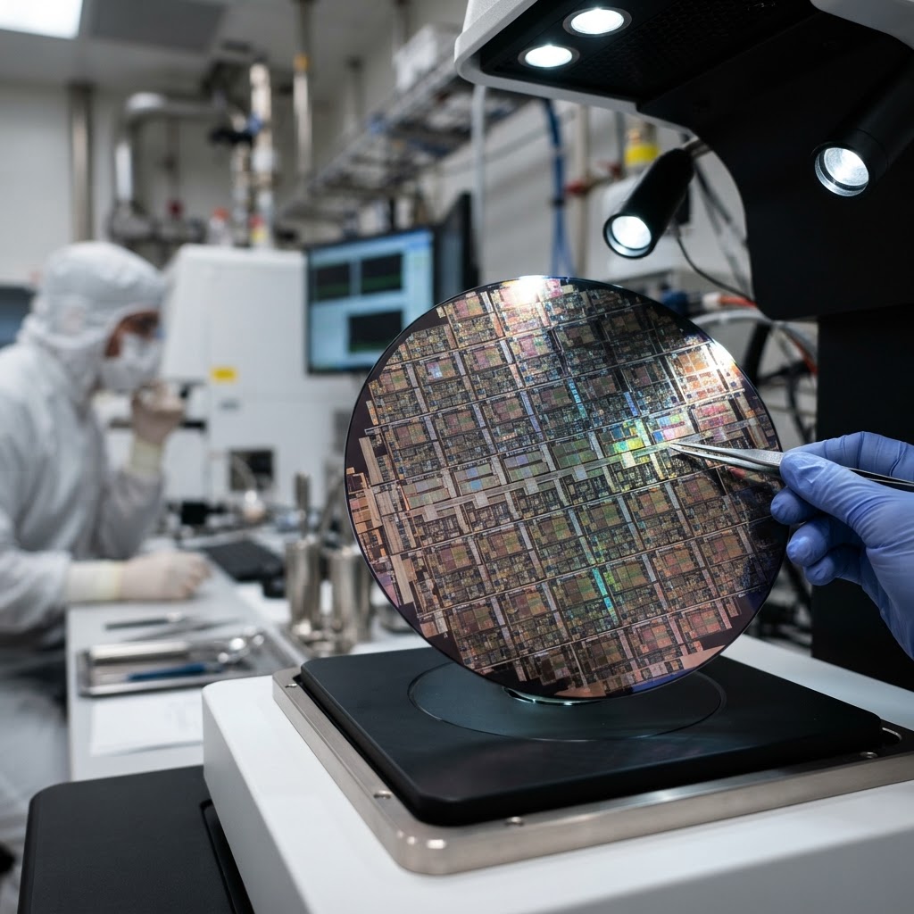
The Chip That Powers Everything — And the Factory That Makes It Possible
In an era where every industrial machine, autonomous vehicle, and data center runs on silicon, the factory that produces chips is arguably the most important building block of the modern economy. Intel's fabrication plants — known as "fabs" — sit at the center of this revolution, combining precision engineering with massive scale to produce billions of transistors on wafers thinner than a human hair.
For manufacturing and industrial companies watching from the sidelines, Intel's fab operations offer a masterclass in what it means to compete at the frontier of process innovation. The lessons embedded in Intel's approach — from capital allocation to workforce strategy — translate directly into frameworks that B2B industrial leaders can apply in their own operations.
This guide breaks down how Intel builds, operates, and markets its semiconductor manufacturing capabilities, and what industrial companies can learn from one of the world's most complex manufacturing environments.
Intel's Fab Network: Scale, Geography, and Capital Commitment
Intel operates one of the largest networks of advanced semiconductor fabs in the world, spanning sites in the United States, Ireland, Israel, and Germany. The company's fab footprint represents decades of capital-intensive investment, with Intel committing approximately $100 billion in planned capital expenditures across its U.S. and European expansion programs through the late 2020s. In 2024, Intel's manufacturing and technology segments absorbed the lion's share of its $25.8 billion in total revenue, underscoring just how central fab operations are to its business model.
The Ohio fab campus — one of the largest semiconductor manufacturing investments in U.S. history — is slated to eventually house eight fab modules on a 1,000-acre site. Even in its early phases, the Ohio project represents a $28 billion commitment, with the first modules expected to reach volume production in the 2026 timeframe. This level of capital deployment puts Intel in a category shared only by TSMC and Samsung in terms of global fab investment.
Intel's Irish campus in Leixlip has been a cornerstone of European chip production, with Fab 34 ramping production using Intel's 4-process node — a critical milestone that demonstrated the company's ability to deliver leading-edge manufacturing outside its U.S. home base. The Leixlip expansion alone required €17 billion in investment, partly supported by EU semiconductor subsidies under the European Chips Act.
For industrial manufacturers assessing their own capital strategies, Intel's approach illustrates a core truth: leadership in precision manufacturing is not achieved through incremental spending. It requires decade-long commitment cycles, geographically diversified production, and the courage to invest through downturns.
Process Node Innovation: The Engine Behind Intel's Competitive Position
Semiconductor manufacturing is defined by the relentless pursuit of smaller, faster, and more energy-efficient process nodes. Intel's Intel 18A process node — expected to enter high-volume manufacturing in 2025 and 2026 — represents the company's most aggressive technological leap in years. Industry analysts from firms including Anandtech and SemiAnalysis have noted that Intel 18A, featuring RibbonFET gate-all-around transistors and PowerVia backside power delivery, places Intel on par with or ahead of TSMC's N2 node in certain performance metrics.
The introduction of Extreme Ultraviolet (EUV) lithography into Intel's production lines has been a defining technical milestone. EUV machines — supplied almost exclusively by ASML — cost upward of $350 million per unit and require purpose-built cleanroom environments to operate. Intel has deployed multiple EUV systems across its Hillsboro, Oregon, and Leixlip facilities, enabling the sub-5nm patterning required for next-generation AI accelerators and client processors.
Yield rates — the percentage of chips on a wafer that meet quality specifications — are the critical performance indicator in fab operations. Intel reported meaningful yield improvements on its Intel 4 process node throughout 2024, which directly enabled higher volumes of Meteor Lake and Lunar Lake processors to reach the market. Every percentage point of yield improvement at scale translates into hundreds of millions of dollars in recovered revenue across a 300mm wafer production run.
For industrial companies operating precision manufacturing lines — whether producing aerospace components, medical devices, or industrial sensors — Intel's investment in process control and metrology offers a powerful analogy. Quality at scale is not an accident; it is the result of obsessive measurement, feedback loops, and continuous engineering iteration applied across every step of the production process.
What B2B Industrial Companies Can Learn From Intel's Manufacturing Playbook
Intel's rise and its ongoing transformation under its IDM 2.0 strategy — which combines internal manufacturing with foundry services for external customers — provides a rich set of lessons for B2B industrial marketers and operators. One of the most important is the power of positioning around capability, not just product. Intel Foundry Services (IFS), launched to compete with TSMC and Samsung for external chip customers, is marketed explicitly on the basis of U.S.-based, secure, advanced-node manufacturing — a capability story that resonates deeply with defense contractors, automotive OEMs, and AI hardware companies.
Content and thought leadership play a central role in Intel's B2B marketing engine. Intel regularly publishes detailed technical white papers, fab tour videos, and engineering blog posts that communicate process node roadmaps directly to procurement engineers and CTO-level buyers. This kind of deep technical content builds trust in markets where purchasing decisions are made over 18- to 36-month cycles and require extensive technical due diligence.
Intel's partner ecosystem strategy — integrating with EDA software providers, equipment manufacturers, and packaging specialists — demonstrates the value of co-marketing with complementary industrial players. For manufacturing companies, developing co-branded case studies and joint go-to-market programs with equipment OEMs or materials suppliers can significantly shorten sales cycles and expand reach into new verticals.
Finally, Intel's transparent communication about manufacturing challenges — including its well-publicized yield struggles on earlier nodes — has paradoxically strengthened customer trust. Industrial B2B buyers respect candor about complexity. Companies that openly discuss their quality journey and improvement roadmaps often build stronger long-term partnerships than those projecting false infallibility.
The Road Ahead: AI, Geopolitics, and the Next Era of Industrial Semiconductor Manufacturing
The semiconductor industry in 2025 and 2026 is being reshaped by two forces above all others: the explosive demand for AI compute infrastructure and the geopolitical imperative to onshore critical manufacturing capacity. Intel is positioned at the intersection of both trends. Its foundry business is actively targeting AI chip customers who need cutting-edge process nodes manufactured in politically stable jurisdictions — a market that Gartner estimates will require hundreds of billions in new fab capacity investment through the end of the decade.
The U.S. CHIPS and Science Act has already disbursed preliminary funding agreements to Intel totaling approximately $8.5 billion in direct grants, with additional loan guarantees extending the total support package. This government backing — mirrored by similar programs in the EU and Japan — signals that semiconductor manufacturing is now a matter of national industrial policy, not just private sector competition.
For industrial companies in adjacent sectors — specialty chemicals, precision equipment, advanced materials — Intel's fab expansion represents a significant demand signal. The construction of a single leading-edge fab requires thousands of tons of ultra-pure chemicals, millions of liters of ultra-pure water, and hundreds of specialized equipment systems. Supply chain partners who align their capabilities with fab builder requirements stand to capture substantial long-term revenue.
The strategic implication for B2B industrial leaders is clear: semiconductor manufacturing is not a distant technology story. It is a procurement opportunity, a partnership ecosystem, and a benchmark for operational excellence. Companies that study Intel's manufacturing model, align their supply chain positioning accordingly, and invest in the technical marketing capabilities to engage engineering buyers will be well positioned to grow alongside the next generation of fab construction.
Start by auditing your current capabilities against the specifications Intel Foundry publishes for its supplier qualification programs — then build your roadmap from there.
Key Takeaways
- Intel has committed approximately $28 billion to its Ohio fab campus alone, making it one of the largest single manufacturing investments in U.S. history and signaling the scale required to compete in advanced semiconductor manufacturing.
- Intel's Intel 18A process node, featuring RibbonFET and PowerVia technologies, is expected to enter high-volume manufacturing in the 2025–2026 window, representing a generational leap in transistor architecture.
- Intel received approximately $8.5 billion in preliminary CHIPS Act grant funding, illustrating how government industrial policy is reshaping capital flows in advanced manufacturing sectors.
- Intel 4 process node yield improvements throughout 2024 directly enabled higher-volume production of Meteor Lake and Lunar Lake processors, demonstrating the direct revenue impact of precision manufacturing quality gains.
Key Quotes
"Our goal is to build the most resilient and sustainable semiconductor supply chain in the world, and that starts with world-class manufacturing." — Pat Gelsinger, Former CEO, Intel Corporation
"The CHIPS Act is a once-in-a-generation opportunity to restore American leadership in semiconductor manufacturing, and Intel is committed to leading that effort." — Gina Raimondo, U.S. Secretary of Commerce
References
- Intel Foundry Services Overview — Official Intel page covering IFS capabilities, process nodes including Intel 18A, and partner ecosystem details
- U.S. Department of Commerce CHIPS Act Funding Announcements — Government source tracking CHIPS and Science Act preliminary memoranda of terms and grant disbursements to Intel and other manufacturers
- ASML Annual Report 2024 — Covers EUV lithography system demand, pricing, and deployment data relevant to Intel's advanced fab operations