NEWS
US Tightens Aviation Component Supplies to China Amid Trade Talks — International FinanceIndia Initiates Sunset Review of Anti-Dumping Duties on TDI Imports — PU DailyPolyurea Industry Briefing: October 5, 2026 — Polyurea MagazineManufacturing Month Spotlights Innovation, Workforce Challenges, and Future Opportunities — Design NewsAbbVie to Participate in Federal — AbbVie News CenterSonderling, NAM, MI Tour Nucor Facility, Talk Investment, Safety and Workforce — NAMAmazon to Double Number of Robotics Manufacturing Facilities — NAMNational Manufacturing Day, 2026 — The White HouseIndustrial Automation: Physical AI Trends — Smart IndustryIndustrial Automation News – Rockwell Automation — Industry TodayManufacturing Week is 2-9 October — InstagramTrilogy Machinery Welcomes New Operations Administrator and Service Technician — The FabricatorUS Tightens Aviation Component Supplies to China Amid Trade Talks — International FinanceIndia Initiates Sunset Review of Anti-Dumping Duties on TDI Imports — PU DailyPolyurea Industry Briefing: October 5, 2026 — Polyurea MagazineManufacturing Month Spotlights Innovation, Workforce Challenges, and Future Opportunities — Design NewsAbbVie to Participate in Federal — AbbVie News CenterSonderling, NAM, MI Tour Nucor Facility, Talk Investment, Safety and Workforce — NAMAmazon to Double Number of Robotics Manufacturing Facilities — NAMNational Manufacturing Day, 2026 — The White HouseIndustrial Automation: Physical AI Trends — Smart IndustryIndustrial Automation News – Rockwell Automation — Industry TodayManufacturing Week is 2-9 October — InstagramTrilogy Machinery Welcomes New Operations Administrator and Service Technician — The Fabricator
Guide

Angstroms and Ambition: How Intel's 18A Process Node Ramp Is Rewriting the Rules of Advanced Semiconductor Manufacturing

How Intel's 18A process node ramp, RibbonFET innovation, and foundry transformation offer manufacturing leaders a blueprint for reclaiming industrial leadership.

Manufacturing UltraOctober 5, 20267 min read
Angstroms and Ambition: How Intel's 18A Process Node Ramp Is Rewriting the Rules of Advanced Semiconductor Manufacturing

At a Glance

AI Summary

How Intel's 18A process node ramp, RibbonFET innovation, and foundry transformation offer manufacturing leaders a blueprint for reclaiming industrial leadership.

Manufacturing UltraOct 5, 20267 min read

Key Takeaways

  • Intel has committed up to $28 billion to its Ohio fab campus, representing one of the largest single domestic manufacturing investments in U.S. history

The Fab Renaissance Nobody Saw Coming

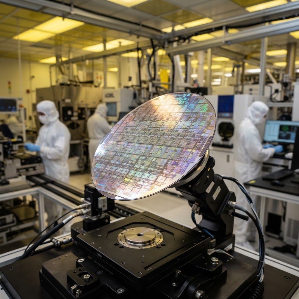
For decades, semiconductor manufacturing was treated as a commodity operation best outsourced to Asia. That assumption is now being dismantled, angstrom by angstrom, inside Intel's network of advanced fabrication plants. Intel is staging one of the most audacious manufacturing comebacks in industrial history.

The stakes could not be higher. Chips now underpin every sector of the global economy, from defense to agriculture to medical devices. Whoever controls leading-edge fab capacity controls the commanding heights of 21st-century industry.

Intel's answer to this moment is the Intel 18A process node, a technology platform the company claims will restore its position at the absolute frontier of transistor density and power efficiency. For manufacturing and industrial leaders watching from the sidelines, the lessons embedded in Intel's strategy are directly applicable to their own operations.

Intel's Global Fab Footprint and the Scale of the Bet

Intel operates major fabrication facilities in Oregon, Arizona, New Mexico, Ireland, and Israel, with new construction underway in Ohio and Germany. The Ohio project, known as Intel Ohio One, represents a planned investment of up to $28 billion and is one of the largest single manufacturing investments in American history. Even in a year of cost restructuring in 2025, Intel maintained capital expenditure guidance in the range of $12 billion to $14 billion for the fiscal year.

The Arizona fabs, specifically the Ocotillo campus in Chandler, are central to the 18A ramp. Intel has been qualifying Intel 18A at Fab 52 and Fab 62, both of which came online as part of a multi-year capacity expansion. These fabs use extreme ultraviolet (EUV) lithography equipment from ASML, with each EUV tool costing approximately $200 million and requiring specialized facilities to operate.

Intel Foundry, the newly restructured external foundry business, reported approximately $4.3 billion in revenue for the first half of 2025 as it worked to attract customers beyond Intel's internal design teams. The company has publicly targeted a path to foundry profitability by 2027, a timeline that depends heavily on successful Intel 18A volume production.

The workforce supporting these operations is enormous. Intel employs roughly 108,000 people globally as of 2025, with a significant share concentrated in manufacturing and process engineering roles. Skilled technician and process engineer hiring has remained a priority even as Intel executed broader headcount reductions in non-manufacturing functions.

Intel 18A: What the Process Node Actually Does and Why It Matters

Intel 18A is the company's most advanced manufacturing process, combining two critical innovations: RibbonFET gate-all-around transistors and PowerVia backside power delivery. RibbonFET replaces the FinFET architecture that has been the industry standard for over a decade, enabling better electrostatic control of the transistor channel at extremely small geometries. PowerVia moves power delivery networks to the back of the wafer, freeing up routing resources on the front side and improving signal integrity.

In benchmark disclosures through 2025, Intel reported that Intel 18A delivers a performance-per-watt improvement of greater than 15 percent compared to Intel 3, the prior leading node. Transistor density on Intel 18A is targeted at approximately 200 million transistors per square millimeter in dense logic cells. These figures place Intel 18A in direct competition with TSMC N2 and Samsung SF2, both of which are also ramping in 2025 and 2026.

The process also supports High NA EUV, the next generation of lithography. Intel was one of the first manufacturers to take delivery of ASML's High NA EUV tool, the TWINSCAN EXE:5000, which prints patterns at a 0.55 numerical aperture compared to 0.33 for standard EUV. This investment positions Intel to extend its process roadmap further into the angstrom era with Intel 14A, already in development.

For industrial companies outside semiconductors, the innovation model here carries a direct lesson. Intel did not simply buy better equipment. It co-developed proprietary architectural innovations (RibbonFET, PowerVia) that are deeply integrated with its manufacturing process.

Sustainable competitive advantage in manufacturing comes from owning the intersection of process know-how and product architecture.

Marketing and Growth Lessons for Industrial Manufacturers

Intel's transformation into a public-facing foundry business required a complete rethinking of its go-to-market approach. For most of its history, Intel sold directly to OEMs and enterprises under a simple brand promise: faster chips inside. The foundry pivot demands a B2B marketing posture that communicates process capability, yield reliability, and IP security to sophisticated design teams at other companies.

Intel has responded by publishing detailed process design kits (PDKs) for Intel 18A, hosting foundry forums with technical deep dives, and establishing a dedicated Intel Foundry customer engagement organization. This is a masterclass in account-based marketing for industrial audiences: lead with engineering credibility, not brand advertising. Industrial manufacturers in sectors like precision machining, specialty chemicals, and contract electronics can apply the same principle by building technical content that speaks directly to the procurement and engineering teams who actually make sourcing decisions.

Transparency about yield and reliability data is another differentiator Intel has leaned into. In a foundry market where TSMC has decades of customer trust, Intel has had to earn credibility through disclosure rather than reputation. Publishing third-party benchmark data, inviting customers into qualification programs, and offering design support services are all tactics that translate directly to industrial B2B sales cycles.

Finally, Intel's ecosystem strategy demonstrates the power of co-investment with key customers. Reports from 2025 indicate that Microsoft has been working with Intel Foundry on a test chip using Intel 18A, while other hyperscaler conversations are ongoing. For industrial companies, identifying two or three anchor customers willing to co-develop a new capability creates both revenue stability and powerful reference case studies for broader market development.

If your company is rethinking its manufacturing value proposition for 2026 and beyond, consider how a co-development partnership with a marquee customer could accelerate both your process roadmap and your credibility in the market.

The Capacity Imperative — F-35 in flight cover
Free Industry Report

The Capacity Imperative

U.S. Advanced Manufacturing in 2027

The Road Ahead: Strategic Implications for the Fab and Beyond

The geopolitical dimension of Intel's manufacturing buildout is impossible to ignore. The CHIPS and Science Act directed approximately $8.5 billion in direct funding to Intel, with the formal agreement finalized in late 2024. This subsidy is not a gift but a strategic instrument: the U.S. government is effectively co-investing in domestic leading-edge capacity to reduce dependence on Taiwan-based fabrication.

For industrial companies across sectors, the lesson is that aligning capital investment plans with national industrial policy goals can unlock substantial non-dilutive funding.

Intel 18A volume production is expected to ramp through 2026, with external customer wafer starts beginning in meaningful quantities during that window. The success of this ramp will determine whether Intel Foundry can credibly compete for the next generation of AI chip, custom silicon, and advanced logic designs that hyperscalers and defense primes are actively sourcing. Analyst estimates from early 2026 suggest Intel Foundry could reach $10 billion in annual external revenue by 2028 if the 18A yield learning curve tracks ahead of internal targets.

The broader semiconductor manufacturing market is projected to grow at a compound annual growth rate of approximately 7 percent through 2030, driven by AI compute demand, automotive electrification, and industrial automation. Intel's ability to capture a meaningful share of this growth depends on executing a manufacturing ramp at a speed and scale that the company has historically struggled with. The organizational and process discipline required to hit that ramp is, in itself, a competitive capability.

For industrial manufacturing leaders, Intel's story in 2025 and 2026 is a live case study in what it takes to re-establish manufacturing leadership after a period of relative stagnation. It requires capital patience, workforce investment, technology co-development, and a marketing organization capable of translating engineering complexity into customer confidence. The companies that master all four dimensions will define their industries for the next decade.

Key Takeaways

  • Intel has committed up to $28 billion to its Ohio fab campus, representing one of the largest single domestic manufacturing investments in U.S. history
  • Intel 18A delivers greater than 15 percent performance-per-watt improvement over Intel 3, positioning it competitively against TSMC N2 and Samsung SF2 in 2025 and 2026
  • Intel Foundry reported approximately $4.3 billion in revenue for the first half of 2025, with a target path to profitability by 2027
  • The CHIPS and Science Act directed approximately $8.5 billion in direct funding to Intel, finalized in late 2024, underscoring the role of policy alignment in large-scale industrial investment

Key Quotes

"Intel 18A is a proof point that Intel can lead in process technology again. The combination of RibbonFET and PowerVia is a genuine architectural leap, not an incremental shrink." — Pat Gelsinger, Former Chief Executive Officer, Intel Corporation

"The availability of a second leading-edge foundry source in the United States is strategically important for the entire semiconductor ecosystem." — Gina Raimondo, Former U.S. Secretary of Commerce

References

The Capacity Imperative — F-35 in flight cover
Free Industry Report

The Capacity Imperative

U.S. Advanced Manufacturing in 2027

Newsletter

Stay in the loop

Get the latest insights on manufacturing marketing, industrial trends, and growth strategies delivered to your inbox.

We'll send you industry insights and manufacturing trends. No spam, unsubscribe anytime.

A massive modern industrial robot arm in a sleek manufacturing facility
Manufacturing Ultra

Marketing for the industrial economy. We help manufacturers, suppliers, and event organizers grow with modern, data-driven programs.

Explore

© 2026 Manufacturing Ultra. All rights reserved.